GOPOWER / GALLIA research consortium - Research
Electronic Defects Study
Deep Electronic Defect identification
Information about defects and their role in determining the doping. Knowledge of the identities and energy positions of shallow and deep levels is critical for further developing devices.
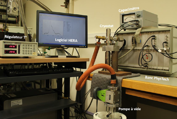
Our the methodology consists to use admittance and capacitance measurement techniques in frequency or transient modes to accede to the spectroscopy (energy, capture cross section, concentration) of shallow (donor (D) or acceptor (A)) levels and of deep levels present in the materials. Admittance spectroscopy versus frequency and temperature give the ionization energy of shallow levels (D or A) introduced by the doping process or intrinsic shallow defects created by growth if any.
Static admittance or capacitance techniques give the free carrier concentration profiles.
Deep levels introduced by intrinsic defects or impurities are generally detrimental for the electronic properties of materials and devices (carrier lifetime…). Those defects will be analyzed by transient of capacitance or current in a DLTS approach on n and p type materials. As the energy range of the DLTS is limited within around 1 eV from the majority carrier band edge and the energy gap of β-Ga2O3 is 4.9 eV, we use photo-capacitance technique such as DLOS (deep level optical spectroscopy) approach in order to accede to deeper energy in the band gap of β-Ga2O3. This DLOS technique was first established in our INL laboratory. The knowledge of optical photoionization cross-section (σopt) given by the DLOS is a unique fingerprint for defect identification in case of transition metal impurities through access to their excited states or in the general case through access to their bond strength in the crystal.
Resistive materials are analyzed by photoinduced current transient spectroscopy (PICTS) thanks to the fixed space charge in such materials.