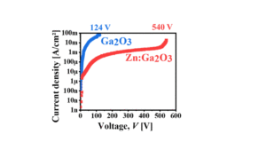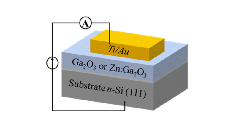
Which the actual critical electrical field of the ultra-wide bandgap semiconductor b-Ga2O3 is? Even that it is usual to find in the literature a given value for the critical field of wide and ultra-wide semi-conductors such as SiC (3 MV/cm), GaN (3.3 MV/cm), b-Ga2O3 (~8 MV/cm) and diamond (10 MV/cm), this value actually depends on intrinsic and extrinsic factors such as the bandgap energy, material residual impurities or introduced dopants. Indeed, it is well known from 1950’s that reducing the residual doping (NB) of the semiconductor layer increases the breakdown voltage capability of a semiconductor media(e.g. as N3=4 by using the Fulop’s approximation for an abrupt junction). A key limitation is, therefore,he residual donor/acceptor concentration generally found in these materials. We report that doping with amphoteric Zinc a p-type b-Ga2O3 thin films shortens free carrier mean free path (0.37 nm), resulting in the ultra-high critical electrical field of 13.2 MV/cm. Therefore, the critical breakdown field can be, at least, four times larger for the emerging Ga2O3 power semiconductor as compared to SiC and GaN. We further explain these wide-reaching experimental facts by using theoretical approaches based on the impact ionization microscopic theory and thermodynamic calculations.